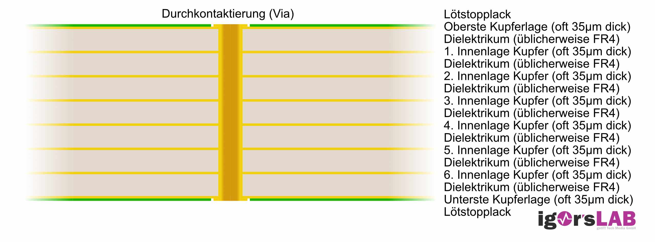
Because they have multiple conductor patterns within them, they’re. This layer contains the bottom side tracks and the bottom side copper pour (if used).
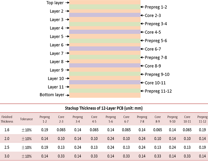
PCB Layer Stack Management
Let's start in the middle and work our way out.
Pcb layers explained. The signal layers include top layer, bottom layer, mid layer 1. In general a pcb is classified by the number of copper layers. These layers get their names coined out from their functions and positions.
These layers are all layers with electrical connections, that is, the actual copper layers. Detailed introduction of different types of pcb layers. The middle layer refers to the middle board layer used for wiring.
However, these special finishes tend to be expensive, and generally only used for commercial products. Even a simple single sided (one layer) board is made up of a conductive metal layer and a substrate layer composited together. In general, a pcb assembly is classified by the number of copper layers.
In the early days of printed circuit board (pcb) manufacturing, the board was simply an insulating core layer, clad with a thin layer of copper on one or both sides. As name suggests, in this type of pcb, a thin layer of conducting material, like copper is applied to both top and bottom sides of the board. Silkscreen, solder mask, copper layer and substrate layer.
Furthermore, the layers explain the comprehensive operation of the pcb. A pcb layer includes signal transferring levels which are vertical to the surface of the pcb. The top layer, also called the component layer, is mainly used.
Signal layers include top layer, bottom layer, and mid layer 1…30. And when you’re ready to generate documentation to share with your manufacturer, your gerbers will be pulling data directly from many of these layers to communicate your design intent clearly. Internal plane layer (ground plane layer) this type of layer is used only for multilayer printed circuit boards and is primarily used to lay out power and ground wires.
Boards that consists of 1 or 2 layers are often called: With many layers of printed circuit boards, designers can make very thick, complex designs which are suitable for a broad range of complicated electrical tasks. These layers are used to indicate a special finish, such as the “hard gold” plating on pcb card connectors.
In pcb, on different layer of board, consist via, which has two pads in corresponding position on different layers. In this video i am explaining different layers of pcb. The layer is covered with wires.
A pcb is the sum total of conductive layers in a proper segmented manner. Layers are a critical component of your pcb design, allowing you to organize a ton of information without cluttering your view. Boards with no copper layers or with more than 2 copper layers are defined and called by the number of copper layers.
Pcb layers explained in a printed circuit board. Like the trifle dessert pictured above, a printed circuit board is made up of multiple layers. They can be made to have over 42 layers;
Layers are a critical component of your pcb design, allowing you to organize a ton of information without cluttering your view. The signal layer is used to complete the wiring layer of the copper foil traces of the printed circuit board. The number of layers used for a pcb depends on the application, the operating frequencies, pin density, and the requirement for signal layers.
And when you’re ready to generate documentation to share with your manufacturer, your gerbers will be pulling data directly from many of these layers to communicate your design intent clearly. Boards that consists of 1 or 2 layers are often called: As the complexity of the pcb increases, so will the amount of layers within.
The meaning of layers in the pcb. Silk screen or solder mask layer are typically applied only to the outer layers of a pcb. Connections are formed in the copper layer (s) as conductive traces by etching away (removing) unwanted copper.
Double layer pcb is also known as double sided pcb. The signal layer is mainly used to arrange the wires on the circuit board. 200 (and higher numbers) these layers are often used as custom user layers, often for imported bitmaps or other eagle scripts.
Boards with no copper layers or with more than 2 copper layers are defined and called by the number of copper layers. This is the inner layer tracks (only for multilayer pcb). The pcb is designed and formed as a stack of layers.
2 layer board and more.
PCB Total Solution ABL Circuits
Rigid PCB Archives DerekPCB

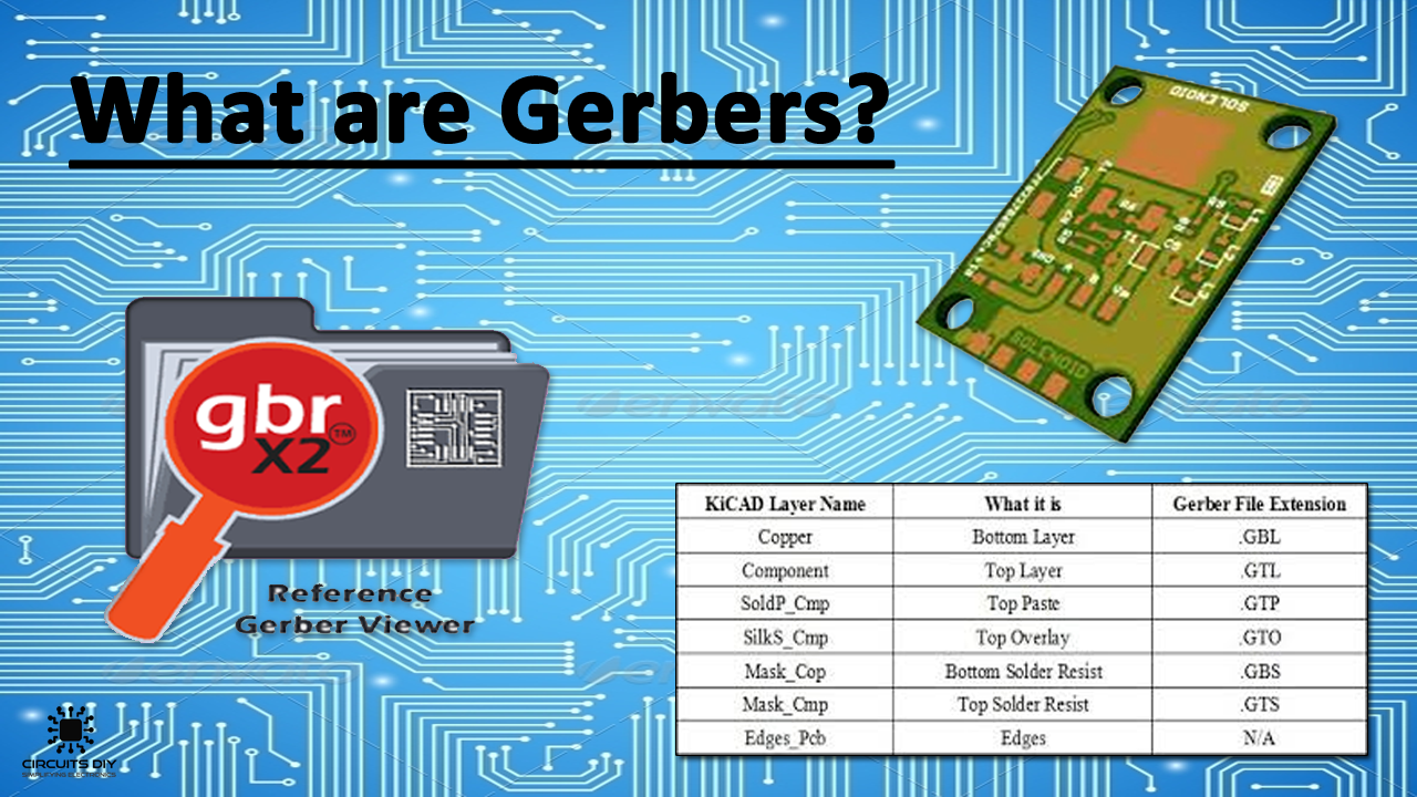
Gerber Files Explained Their Role & Need in PCB Manufacturing

What is PCB board ?Explained (tamil)........ YouTube
pcb layers What are these black strips on PCB
Rigid PCBs ABL Circuits

Double Sided Pcb Design Orcad PCB Designs

3 options of 16L PCB stack up Weller PCB
TCL Elektronika Heavy Copper PCBs
4 Layer Pcb Design Rules PCB Designs
PCB LayersFundamentals And Simple Introducing WellPCB
From the schematic to the finished PCB layout generally

Eagle Pcb Mounting Holes / Every Layer Explained In
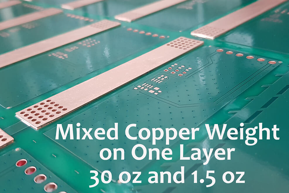
Heavy Copper PCBs DKDaleba

PCB Manufacturing Process How are PCB Made Process
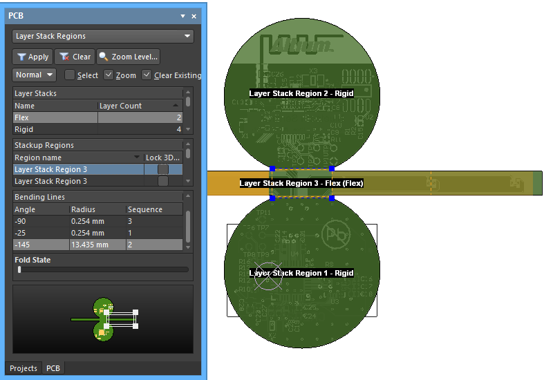
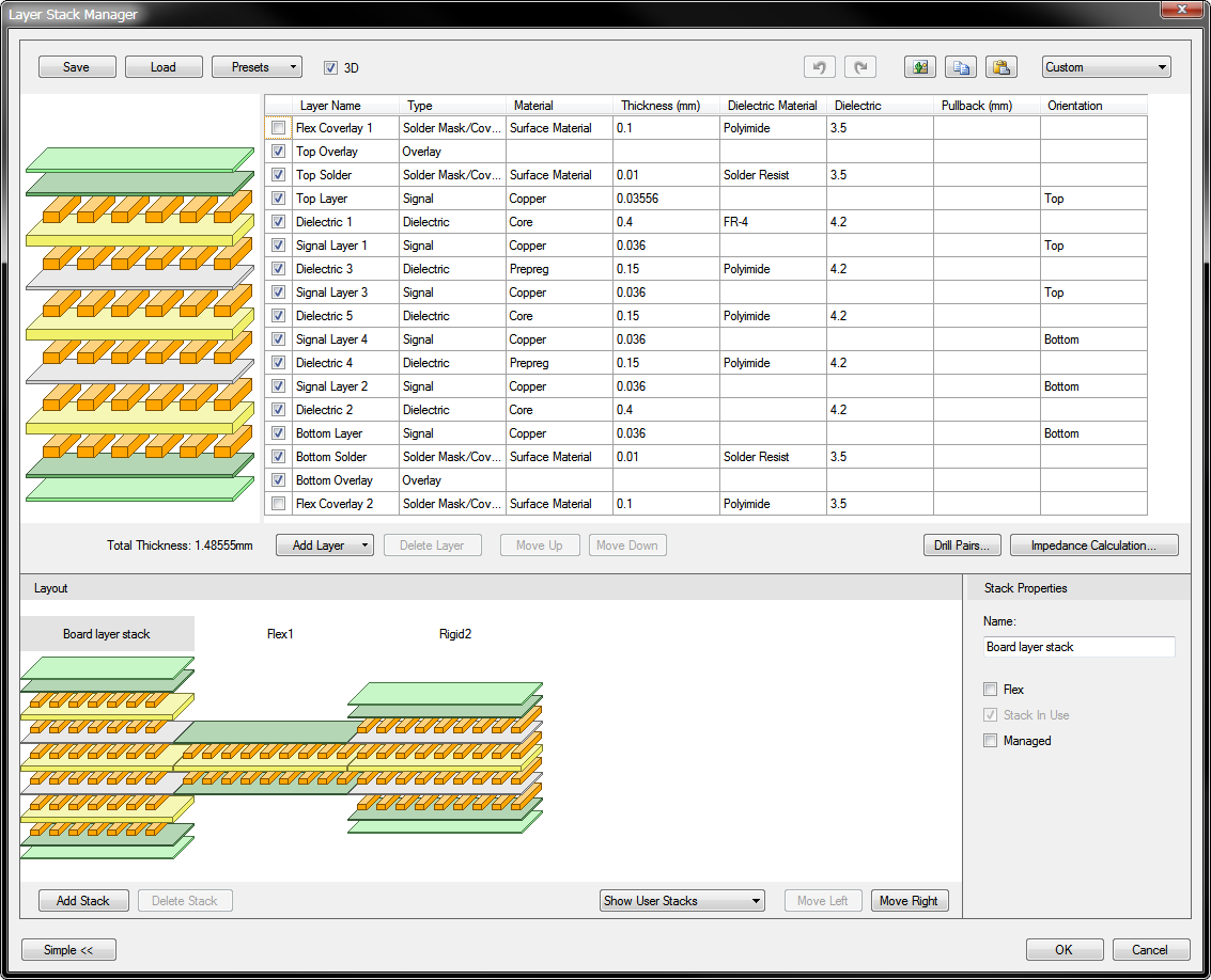
PCB Layer Stack Regions Altium Designer 18.0 User

What are PCB layers pcbknow
4 layers pcb board What is importance of copper in 4

4 Layer Pcb Design Rules Design Pcbs For Emi Part 2


